|
|
BMe Research Grant |
|
Doctoral School of Physics
Department of Physics/Institute of Physics
Supervisor: Dr. Halbritter András
Study of nanometer-sized graphene-SiOx resistive switches
Introducing the research area
The goal of my research is to fabricate and study nanometer-sized (< 10 nm) resistive switches. I examined the electrical properties of a SiOx based resistive switch, especially dead time, which is not typical of the memristive systems. The switching regions were formed between two graphene electrodes with 1-3 nm spacing.
Brief introduction of the research place
My
research work is carried out in the
Atomic and
Molecular Electronics Research Group of the Physics Department.
The research field of the group is the investigation of transport phenomena of
nanometer-scaled atomic and molecular contacts. The presented research was
carried out in collaboration with
Department of Physics, University of Basel
and
Microtechnology Department of the Institute of Technical Physics & Material
Sciences.
History and context of the research
The resistive switch or memristor [2] is a passive electronic device whose resistance can be reversibly controlled by applying voltage between its two terminals [1]. Typically, it can be programmed at higher voltage, while its states can be read noninvasively at low signal level. According to the polarities of the write and erase voltages the devices can classified into bipolar (opposite polarity) or unipolar (same polarity) switches (see Figure 1) [3].
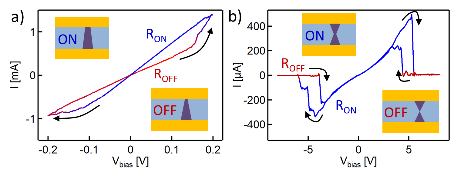
Figure 1: Typical switching curves for a) bipolar [S4] and b) unipolar [S3] devices. The insets show possible structures of the conductive filament.
Generally, the resistive switches are realized by a 10-100 nm thick insulator film sandwiched by two electrically conductive electrodes. Applying appropriate electric field conductive filament can be formed inside the insulator layer. During the resistance transition the diameter of the filament is tuned (insets of Figure 1), whose size is in the range of a few nanometers [4,5]. Thereby the device can be scaled to very small size [6]. The fast and non-volatile properties make them more effective memories (RRAM) than the current CMOS type ones. The resistance of some kind of memristors can be tuned almost continuously, which allows to create analog memories or artificial neural networks from them [7].
The research of RRAM covers wide range of topics like materials, switching mechanisms, manufacturing, integration or special functions [3]. Although it is intensively researched field by large corporations in semiconductor industries, such as HP, IBM, Samsung, TSCM, there is still no material combination which would have overcome any others.
The research goals, open questions
The semiconductor device fabrication will reach the 10 nm spatial resolution soon. On such a small scale the quantum mechanical effects, such as quantum tunneling, limit the operation of the current CMOS devices [8]. In order to sustain Moore-law we need electrical components which exploit the different behavior of the material in nanoscale. The resistive switches are promising candidates, but their achievable smallest size has not been clarified yet.
Besides the device fabrication, formation of stable electrical contacts is also challenging since electrodes with similar spacing (<10 nm) is needed. This is below the current lithography resolution. The surface diffusion of some metals could have significant effect in nanoscale which makes it difficult to establish stable electrical contact [9]. Using graphene as the electrode can provide a solution since it has atomic stability due to the strong covalent bonds.
A possible way to create nanometer sized gap is to break electrically an initially continuous wire made by lithography process (Figure 2.a). In case of metals this method is called electromigration and is already a proven technique. However, for graphene there have been only some initial measurements, and the exact mechanisms were not investigated in detail. Prior to our study the nanogap formations were performed on small, multi-layer graphene which is not ideal for application [10].
Finally, we examined in more detail a confusing effect of SiOx switch, which had already been observed by other groups but not was explained as yet. Despite the unipolar nature of SiOx switch, both states can be stored and read at low signal level [11].
Methods
Sample fabrication
The graphene sheets were grown by chemical vapour deposition (CVD) on copper foil at the University of Basel. The graphene is single layer, polycrystalline and few cm2 in size. After etching the copper foil the graphene was transferred onto Si substrate covered by SiO2 or Si3N4. The graphene was tailored by Ar/O2 plasma etching and the metal pads were deposited by electron beam evaporation. Prior to these steps the required masks were defined by electron-beam lithography. The width of the narrowest part was varied between 100 – 600 nm. During one sample fabrication process hundreds of samples can be created, so we can perform statistical analysis.
Measurement techniques:
The electrical measurements were performed by a measurement control software implemented in C#. It can communicate with the National Instruments data acquisition card, oscilloscope or function generator connected to the computer.
Fabrication of graphene nanogap
The breakdown process of the graphene is based on ramping of the bias voltage (Vbias) on the sample, while the current is monitored frequently (Figure 2.a-b). When narrowing of the graphene stripe begins the current drops suddenly and the bias voltage has to be removed quickly, otherwise the gap being formed gets too wide. In order to get more reliable control voltage pulses were applied whose amplitudes were increased after each cycle. The oxidation of carbon atoms is the proposed mechanism of the breakdown under ambient conditions.
The few nanometer sized gaps can be characterized by electrical measurement based on quantum tunneling effect. The gap can be described by a potential barrier and its height (Φ) and width (d) can be extracted from the I-V measurements (Figure 2.c) [12]. During my visit in Basel AFM and SEM measurements (Figure 3.a) were also performed. For more accurate characterization, I performed electrical measurements at the temperature of liquid helium (4.2 K).
In order to study the effects of the environment, I performed statistical analysis both in air and vacuum (< 1 · 10-6 mbar). To investigate the role of the insulator layer under the graphene I worked with SiO2 and Si3N4 substrates.
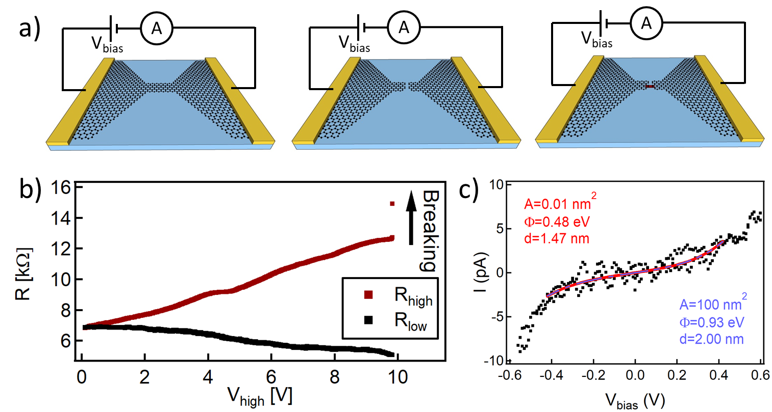
Figure 2: a) Illustration of the steps of forming nanometer-sized SiOx switch. b) The resistance at low (black) and high (red) voltage level during the process of the electrobreakdown. c) Electrical characterization of the nanogap assuming different junction areas (A).
Examination of SiOx switch
The active region of SiO2 switch is confined under the 2 nm wide gap (Figure 2.a). When voltage (8-10 V) is applied to the two sides of the nanogap, a crystalline, silicon rich conduction channel evolves due to the large electric field (> 109 V/m) [13]. It connects electrically the two sides again. This filament can be destroyed by high voltage (6 V) due to the Joule-heating or formed again using lower voltage (4 V) (see on Figure 1.b). Depending on the speed of the driving voltage I used data acquisition card or function generator as a voltage source. The shortest transition was 50 ns, which was an instrumental limit. The switching effect of SiOx can be examined solely in vacuum, because without any passivation layer the surface gets oxidized.
Results
We demonstrated a controlled and reproducible fabrication of sub-5 nm wide gaps in single-layer graphene electrodes with high yield (> 95%). The use of CVD graphene allows the production of a large number of devices. The gap size, obtained from statistical analysis, ranged from 0.3 nm to 2.2 nm and their resistances were in the desired range (Figure 3.b). The measurement under ambient and vacuum condition revealed significant difference; in oxygen rich environment in most cases the tunnel current was not measurable. It refers to larger (> 5 nm) gap size (Figure 3.b, Fail) [S1].
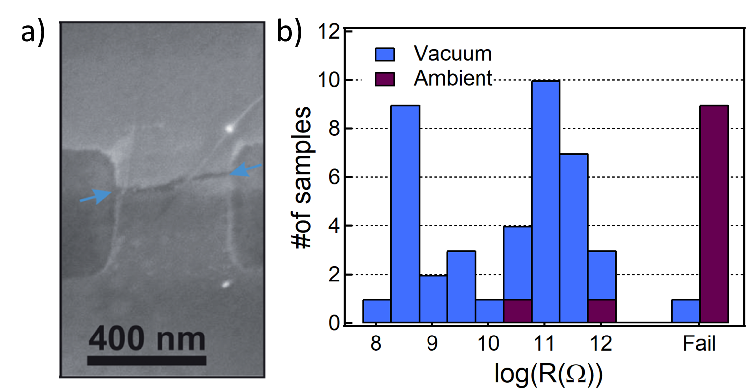
Figure 3: a) A SEM image of the graphene
constriction after EB. b) Statistical results of the EB process for vacuum and
ambient conditions
[S1].
In order to study the effect of environment I performed systematic measurements, where the electrical power at the moment of the breakdown was examined as the function of pulse length (τ=5 μs-5 s) and environment (ambient air, vacuum, SiO2 and Si3N4 substrate). Calculating the number of oxygen molecules hitting an atomic site during a single pulse, there is always enough oxygen to oxidize the carbon in ambient air and never enough in vacuum (Figure 4). Therefore, the breakdown process can be examined in two, significantly different regimes.
The measurements revealed that in vacuum much higher power is needed than in ambient air. Furthermore we have observed a tendency that on average a higher power was required to break a junction if short pulses was applied. By rescaling the power to temperature (T), using a thermal model, the measured data on 1/T-log(τ) graph show linear tendencies (Figure 4). Assuming a thermally activated process behind the breakdown the slope of the lines gives the activation energy. Significantly different values were obtained for the two regimes. Under ambient conditions the activation energy suggests the oxidation of carbon atoms, while in vacuum sublimation is the proposed mechanism. The substrates did not essentially affect the breakdown process [S2].
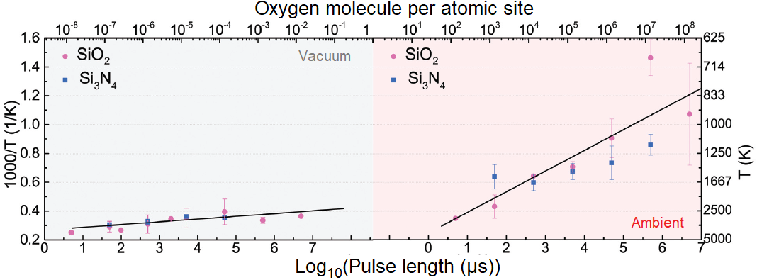
Figure 4: The estimated temperature at the moment of the breakdown as the function of the pulse length [S2].
Since the electroforming of SiOx is electric field driven, it can be assumed that the active region is similar in size to the nanogap (1-3 nm) (see Figure 2.a). So far it has not been shown that this resistive switch system can function in such a small size. According to my observations there were no significant differences compared to the results of other groups [S3].
I have demonstrated that the device operation is governed by multiple physical time scales. The resistance change does not occur right after the switching voltage is applied, but after a time delay (τset, τreset), which is common in resistive switches. It can be tuned exponentially with the bias voltage. Furthermore, the transition do not follow gradual crossover, rather sudden jump within a short switching time (τswitch). Finally, there is another timescale which is not typical of the memristive systems, the dead time (τdead). Once the device is switched OFF, it is blocked in the OFF state for a time period (dead time), even if the driving signal would be sufficient for a set transition. The length of dead time shows strong temperature dependence, but does not depend on the driving condition.
In the case of unipolar switching it is the dead time that enables that both states be stored and read at low voltage by the proper choice of the unipolar pulse sequences. Without a dead time the contact would always switch back to low resistance state after the reset pulse, when the driving voltage falls to zero [S3].
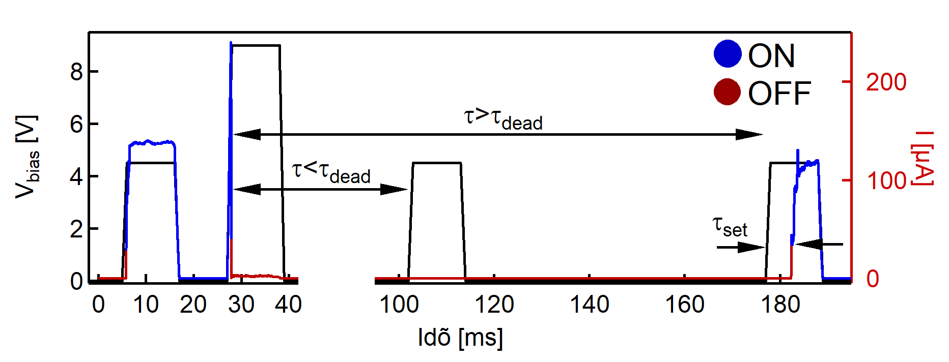
Figure 5: Illustration of timescales in SiOx switches. τswitch and τreset are under the time resolution of this measurement. The colored parts correspond to ON (blue) and OFF (red) states [S3].
Expected impact and further research
One of the most promising applications of resistive switches is the implementation of neural networks, where each synapsis would be realized by a resistive switch [7]. Since they can be switched fast, exhibit non-volatile behavior and show high endurance, new type of memories can be created, for example the Storage Class Memory filling the gap between DRAM and FLASH memory [14]. It is also possible to use them as logical gateways to enable the implementation of a computer other than the Neumann architecture [15].
Currently, various resistive switching systems, which were examined in AFM setup by our group, (Ag2S, Nb2O5, VO2, V2O5) are being implemented by lithographic technique. These samples would have higher stability. We have already demonstrated the role of the asymmetry of the electrodes in Ag2S memristors made by lithography [S4]. There are ongoing investigations on the dead time including the possibility to tune it and observe it in other memristive systems.
Publications, references, links
List of corresponding own publications
[S1] Cornelia Nef, László Pósa, Péter Makk, Wangyang Fu, András Halbritter, Christian Schönenberger, Michel Calame. High-yield fabrication of nm-size gaps in monolayer CVD graphene. Nanoscale 6:(13) pp. 7249-7254, (2014)
[S2] El Abbassi Maria, Posa Laszlo, Makk Peter, Nef Cornelia, Thodkar Kishan, Halbritter Andras, Calame Michel. From electroburning to sublimation: substrate and environmental effects in the electrical breakdown process of monolayer graphene. Nanoscale 9:(44) pp. 17312-17317, (2017)
[S3] Pósa László, El Abbassi Maria, Makk Péter, Sánta Botond, Nef Cornelia, Csontos Miklós, Calame Michel, Halbritter András. Multiple Physical Time Scales and Dead Time Rule in Few-Nanometers Sized Graphene–SiOx-Graphene Memristors. Nano Letters 17:(11) pp. 6783-6789. (2017)
[S4] A Gubicza, D Zs Manrique, L Pósa, C J Lambert, G Mihály, M Csontos, A Halbritter. Asymmetry-induced resistive switching in Ag-Ag2S-Ag memristors enabling a simplified atomic-scale memory design. Scientific Reports 6: Paper 30775. 9 p. (2016)
Table of links
Semiconductor device fabrication
List of references
[1] Leon O. Chua, Memristor - The Missing Circuit Element, IEEE Transactions on circuit theory, vol. ct-18, no 5. (1971).
[2] Leon Chua, Resistance switching memories are memristors. Applied Physics A, 102(4):765–783 (2011).
[3] Jae Sung Lee, Shinbuhm Lee, and Tae Won Noh, Resistive switching phenomena: A review of statistical physics approaches. Applied Physics Reviews 2, 031303 (2015)
[4] Yuchao Yang, Peng Gao, Siddharth Gaba, Ting Chang, Xiaoqing Pan & Wei Lu, Observation of conducting filament growth in nanoscale resistive memories. Nature Communications volume 3 (2012).
[5] A. Geresdi, M. Csontos, A. Gubicza, A. Halbritter and G. Mihály, Fast operation of nanometer-scale metallic memristors: highly transparent conductance channels in Ag2S devices. Nanoscale, 6, 2613 (2014).
[6] Geoffrey W. Burr et al., Overview of candidate device technologies for storage-class memory. IBM Journal of Research and Development, 52 449-464 (2008).
[7] Geoffrey W. Burr et al., Neuromorphic computing using non-volatile memory. Advances in Physics: X, 2, 89−124 (2017).
[8] V. V. Zhirnov, R. K. Cavin, J. A. Hutchby and G. I. Bourianoff, Limits to binary logic switch scaling - a gedanken model," in Proceedings of the IEEE, vol. 91, no. 11, pp. 1934-1939 (2003).
[9]
F. Prins,T. Hayashi, B. J. A. de Vos van Steenwijk, B. Gao, E. A. Osorio, K.
Muraki,
and H. S. J. van der Zant, Room-temperature stability of Pt nanogaps formed
by self-breaking, Appl. Phys. Lett. 94, 123108 (2009).
[10] Ferry Prins et al., Room-temperature gating of molecular junctions using few-layer graphene nanogap electrodes. Nano Letters, 11, 4607-4611 (2011).
[11] Jun Yao, Jian Lin, Yanhua Dai, Gedeng Ruan, Zheng Yan, Lei Li, Lin Zhong, Douglas Natelson, James M. Tour, Highly transparent nonvolatile resistive memory devices from silicon oxide and graphene. Nature Communications volume 3 (2012).
[12] John G. Simmons. Generalized formula for the electric tunnel effect between similar electrodes separated by a thin insulating film. Journal of Applied Physics, 34 (6):1793–1803 (1963).
[13] Jun Yao, Lin Zhong, Douglas Natelson & James M. Tour, In situ imaging of the conducting filament in silicon oxide resistive switches. Scientific Reports 2, (2012).
[14] R. F. Freitas and W. W. Wilcke. Storage-class memory: The next storage system technology. IBM Journal of Research and Development, 52(4.5):439–447, (2008).
[15] Julien Borghetti, Gregory S. Snider, Philip J. Kuekes, J. Joshua Yang, Duncan R. Stewart, R. Stanley Williams, ‘Memristive’ switches enable ‘stateful’ logic operations via material implication, Nature 464, 873–876 (2010).
