|
|
BMe Research Grant |
|
Doctoral School of Physics
Department of Atomic Physics/Institute of Physics
Supervisor: Dr. Gali Ádám
Theoretical investigation of solid state quantum bits
Introducing the research area
Nowadays, we are living the revolution of quantum technology. By applying quantum computers, the time of certain operations can be reduced by orders of magnitudes, whereas the introduction of quantum communication can largely improve cryptography of quantum information. An important building block of quantum information processing is the quantum bit (or qubit) and these qubits are the operational units for storing and transmitting quantum information – similarly to bits in classical computers. Physical representations of qubits are two-level quantum systems manifesting in various realizations. One such realization can be paramagnetic point defects embedded in solid states [1], where information is encoded in nonzero spin state. The host material must be a wide band gap semiconductor, and the point defect has to introduce deep levels in the band gap. These requirements are fulfilled by certain point defects incorporated in silicon carbide (SiC) that proved to be very promising for quantum technology applications. During my research, I have carried out theoretical investigations on paramagnetic point defects in SiC by means of modern electronic structure calculation methods.
Brief introduction of the research place
I carry out my research as a member of Semiconductor nanostructures “Lendület” Research Group (principal investigator: Dr. Ádám Gali) at the Department of Atomic Physics, BUTE and at the Wigner Research Centre for Physics, HAS. Calculations requiring high computational capacities are carried out on computer clusters maintained by the group and by the National Information Infrastructure Development Institute, using the Vienna Ab Initio Simulation Package (VASP) [2].
History and context of the research
The subject of my research the investigation of point defects in SiC, which can be considered potential candidates for quantum technology applications. Point defects can be formed by an incorporated single external atom residing at a lattice site replacing a Si or C atom (substitutional point defect), or an empty lattice site (Si or C vacancy), but even multiple neighboring point defects and/or vacancies (defect complex) can form a qubit. The most famous member of this family is the so-called nitrogen-vacancy defect in diamond [3] consisting of a substitutional N atom at a C site and an adjacent Si vacancy. In particular, the qubit state is realized by the single negative charge state exhibiting S = 1 spin state, and hence this particular charge state is referred to as NV center. The spin state can be manipulated by laser light of a certain wavelength even at room temperature (optical spinpolarization) allowing information encoding and readout all-optically. Despite their unique success, NV centers exhibit disadvantageous properties as well, namely the wavelength of the optical readout falls far from the near-infrared (NIR) region what is undesirable in respect of quantum communication; on the other hand, integration of diamond into the currently available semiconductor devices is not straightforward. Notwithstanding, SiC is a technologically mature material with superior properties hosting promising quantum bit candidates exhibiting NIR emission.
The research goal, open questions
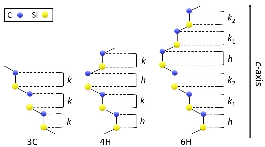
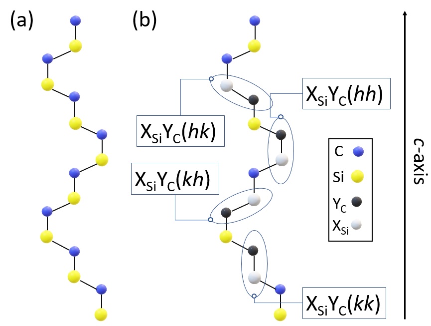
SiC is a polytypic material, i.e. it forms various crystal structures. The most common polytypes of SiC are 3C, 4H and 6H SiC (Figure 1). As a result of polytypism, lattice sites in SiC exhibit different symmetries depending on the local environment: a lattice site can show hexagonal (h) or cubic (k) local symmetry allowing a point defect to form various defect configurations (Figure 2).

Figure 1: Unit cells of technologically important SiC polytypes. Polytypes consist of Si-C dual atomic layers comprising lattice sites exhibiting hexagonal (h) or cubic (k) local symmetry as indicated. In the case of more h/k bilayers, layers with identical symmetry are distinguished by introducing numbering in the notations. Crystal axis (c-axis) is perpendicular to the plain of bilayers.
It is reasonable to study the NV center incorporated by SiC because it is expected to exhibit similarly promising properties than its diamond-embedded counterpart. I have investigated magnetic and optical properties of NV center in SiC along with the conditions of its formation and application in quantum technology. Divacancy in SiC is a defect complex consisting of neighboring Si and C vacancies (Figure 2) exhibiting NIR emission [4] (such as NV center in SiC). Furthermore, optical spinpolarization has been demonstrated on divacancy [5] suggesting that divacancy in SiC is a promising qubit candidate. On the other hand, the divacancy related photon emission (photoluminescence) appears upon excitation energies above an unexpectedly high energy threshold, while below the photoluminescence is quenched as observed in experiments [S3, S4]. According to the established physical model [S4] divacancy is present in its single negative charge state upon excitation energies below the observed threshold; however the qubit state is realized by the neutral charge state. My results support the established microscopic model for the quenching mechanism; furthermore, based on my results we have managed to elaborate a protocol for charge state control and simultaneous excitation of the neutral divacancy that is crucial for the qubit manipulation.

Figure 2: (a) Lattice structure of perfect 4H SiC crystal and (b) defective 4H SiC hosting defect complexes comprising two adjacent defect atoms (XSi, YC) or vacancies with all possible defect configurations. In case of XSi = VSi and YC = NC the nitrogen-vacancy defect configurations, while with the addressing of XSi = VSi és YC = VC divacancy defect configurations can be obtained. In brackets local symmetries of defect sites are denoted, respectively.
Methods
For the atomic electronic structure calculations I applied the ab initio density functional theory (DFT) along with the so-called Born-Oppenheimer (BO) approximation. In the BO approximation electrons are considered to move independently from the nuclei owing to the significant difference between the electronic and nuclear mass that allows determining the electronic structure for arbitrary nuclear configuration. In this way, the minimum energy of the system corresponds to the nuclear configuration yielding the minimal total electronic energy. This nuclear configuration is referred to as relaxed geometry. Note that in cases when electrons are strongly coupled to the nuclear movement, i.e. to lattice vibrations (phonons), BO approximation may fail in describing the system correctly. DFT is based on the independent-particle approximation, i.e. the energy levels can be determined separately for every single electron. However, since electrons are treated as non-interacting quasiparticles, the obtained eigenenergies bear no explicit physical meaning.
I have studied the point defects in bulk SiC; hence selecting the so-called supercell method for the modeling of the defective system is a natural choice. The supercell contains integer number of unit cells in each directions and the point defect is placed in the center of it (Figure 3). During the calculation, three-dimensional infinite tiling of the supercell is applied using the periodic boundary conditions. Hence a supercell size had to be chosen that is big enough to neglect the interaction between the defect and its images. However, due to the long range Coulomb interaction between electrically charged defects, infinite supercell should be used that is obviously inapplicable. Therefore, the resultant artificial energy contributions are treated with so-called charge correction schemes [6]. In the case of the studied point defects, applying ~500 atom supercells resulted in reasonably accurate results.

Figure 3: Supercell of defective SiC with a single point defect in the center that is a substitutional defect in this case. The red blur indicates the NIR emission of the point defect that is highly desirable with respect to quantum technology applications.
By means of the employed methods, energy of optical transition between the ground and first excited states can be calculated. This transition is called zero-phonon line (ZPL) since electron-phonon coupling is not considered in this case. Defect formation can also be addressed by the calculation of formation energies as well as the so-called charge transition levels, which are positions of the Fermi level where formation energies of two charge states are identical. In addition, the possibly emerging magnetic splittings in the electronic structure can also be determined as the hyperfine splitting arising from the interaction of the electronic and nuclear spins, the zero-field splitting (ZFS) originating from the electron spin - electron spin interaction and the spin-orbit splitting resulting from the interaction electron spin and angular moment. Magneto-optical properties are not only important with respect to the applications, but they also provide the fingerprint of the corresponding point defect allowing unambiguous defect identification by comparing theoretical results and experimental data.
Results
Recently, 4 unidentified ZPL lines have been observed in nitrogen-doped 4H SiC samples in the NIR region in the corresponding photoluminescence (PL) spectrum [S5, S8]. Data obtained from electron paramagnetic resonance (EPR) measurements are also available for the same point defect that can be the origin of the unidentified ZPLs [S5, S8]. Based on the calculated ZPLs, the hyperfine and ZFS constants, I identified the corresponding point defect as the NV center that can form 4 different defect configurations in 4H SiC (Figure 2). Furthermore, I calculated the formation energies of the NV center configurations along with other defects that would be formed in case of sample preparation at thermodynamic equilibrium [e.g. chemical vapor deposition (CVD)] in the 4H polytype that allowed the estimation of defect concentrations (Figure 4). Based on my results it turned out that, among the considered point defects only one spin active defect exceeds the concentration of the NV center by about 7 orders of magnitude and it is the substitutional N point defect at a C site establishing an undesirable dense spin bath. Another usual sample preparation process is ion implantation. In this case, large amount of N point defects along with Si and C vacancies are formed. During the subsequent annealing they become mobile and may bond with each other yielding NV centers and divacancies. Based on my calculations, additionally to the NV centers, neutral divacancies (with S = 1 spin sate) are always formed in the 3C, 4H and 6H polytypes – and this was confirmed by experimental observations. Furthermore, divacancy is optically active in the excitation region of NV center that may be strongly detrimental for the photostability of the NV center. In summary, for the fabrication of NV centers other sample preparation processes should be sought after. Nevertheless, I note that at sufficiently N-doping concentration the amount of NV centers can be increased in case of samples prepared by ion implantation [S5-S8].

Figure 4: Concentrations of the studied point defects in case of N-doped 4H SiC samples prepared with CVD. Point defects from left to the right: substitutional N defect, Si vacancy, C vacancy, C antisite - vacancy pair, divacancy and Si vacancy surrounded by different number of substitutional N defects [S5].
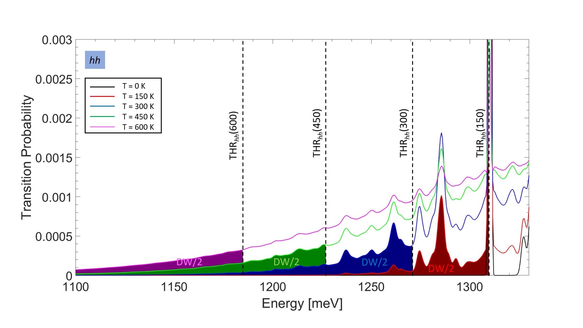
Similarly to the NV center, divacancy can also form 4 different defect configurations in 4H SiC (Figure 2). During my research, I have studied the divacancy related PL quenching, as mentioned before. According to the microscopic model, upon reaching the excitation threshold energy the single negative charge state of the divacancy transforms to a neutral charge state, i.e. it is re-ionized and along with this the PL signals of the neutral charge state are recovered. The re-ionization of the negative charge state can be achieved by promoting an electron from the highest occupied gap state to the conduction band (CB). The required energy can be estimated by the energy gap between the 0/- charge transition level and the CB minimum. By comparing the calculated results for all 4 divacancy configurations with the experimental excitation threshold energies I have found good agreement supporting the established microscopic model. Charge state control and the simultaneous excitation of the neutral divacancy using only a single laser is of high importance. Since the corresponding excitation energies are lower than the excitation (or re-ionization) threshold energies, the key would be raising the temperature to create phonons. In this way, the lower excitation energies generally used (~1.27 eV) can be completed by phonon energies that can be enough for the charge state control. Based on the calculated results, the re-ionization at room temperature (~300 K) can be carried out with significant probability (Figure 5), similarly to the excitation of the neutral charge state, i.e. the qubit manipulation [S3, S4].

Figure 5: Calculated PL spectrum of the hh divacancy normed to 1, i.e. the one-electron transition probability causing the re-ionization with respect to the optical excitation energy. Colored areas indicate the cumulative transition probability that is set to the half of the so-called Debye-Waller (DW) factor. DW factor is the magnitude of the area locked in by the ZPL and hence the cumulative transition probability in case of an excitation in the position of ZPL at zero temperature is DW/2. It can be seen that at around 300 K, the divacancy can be re-ionized with remarkably probability.
Expected impact and further research
The obtained results may significantly contribute to the application of point defects as qubits. Furthermore, these systems can be applied as biomarkers in medical sciences [7], and as building blocks of ultrasensitive nanosensors [8]. Further goals of my research encompass the investigation of transition metal (TM) point defects - particularly vanadium and molybdenum - in SiC which are also promising candidates for single-photon sources in quantum communication or quantum memories based on preliminary theoretical and experimental studies [S2, 9]. Understanding the nature of the rich physics exhibited by TM atoms owing to their strongly correlated d-orbitals is crucial for the mentioned applications. In characterization and in discovering further point defects atomistic simulations may play an important role as have done so far providing pioneer results in this field.
Publications, references, links
List of corresponding own publications
[S1] A. Csóré, A. Gali, “Ab initio study on highly anisotropic magnetic properties of Kramers doublet systems”, in preparation
[S2] L. Spindelberger, A. Csóré, G. Thiering, S. Putz, N. T. Son, R. Karhu, J. Ul Hassan, T. Fromherz, A. Gali and M. Trupke, Optical Properties of Vanadium in 4H Silicon Carbide for Quantum Technology, accepted at the Phys. Rev. A (IF: 4.782), arXiv: 1901.05371 (2019)
[S3] A. Csóré, B. Magnusson, N. T. Son, A. Gällström, T. Ohshima, I. G. Ivanov, A. Gali, First-principles study on photoluminescence quenching of divacancy in 4H SiC, Materials Science Forum, accepted
[S4] B. Magnusson, N. T. Son, A. Csóré, A. Gällström, T. Ohshima, A. Gali and I. G. Ivanov, Excitation properties of the divacancy in 4H-SiC, Phys. Rev. B 98, 195202 (2018), IF: 3.813
[S5] A. Csóré, H. J. von Bardeleben, J. L. Catin, A. Gali, Characterization and formation of NV centers in 3C, 4H and 6H SiC: an ab initio study, Phys. Rev. B 96, 085204 (2017), IF: 3.813
[S6] A. Csóré, Electronic structure and magneto-optical properties of NV centers in 4H and 6H SiC, Proceedings of the PhD workshop of the Physics Doctoral School at the Faculty of Science, pp. 21-24. (2017), IF: -
[S7] A. Csóré and Á. Gali, Density functional theory on NV center in 4H SiC, Mat. Sci. For., Vol. 897, pp. 269-274 (2016), IF: -
[S8] H. J. von Bardeleben, J. L. Cantin, A. Csóré, A. Gali, E. Rauls, U. Gerstmann, NV centers in 3C, 4H, and 6H silicon carbide: A variable platform for solid-state qubits and nanosensors, Physical Review B 94, p. 121202 (2016), IF: 3.813
Table of links
Semiconductor Nanostructures “Lendület” Research Group
Department of Atomic Physics, BUTE
Wigner Research Centre for Physics, HAS
Density Functional Theory (DFT)
Born-Oppenheimer (BO) approximation
List of references
[1] J. R. Weber, W. F. Koehl, J. B. Varley, A. Janotti, B. B. Buckley, C. G. Van de Walle and D. D. Awschalom, Quantum computing with defects, Proc. Natl. Acad. Sci. USA 107, 8513 (2010)
[2] G. Kresse and J. Furthmüller, Efficient iterative schemes for ab initio total-energy calculations using a plane-wave basis set, Phys. Rev. B 54, 11169 (1996)
[3] M. W. Doherty, N. B. Manson, P. Delaney, F. Jelezko, J. Wrachtrup and L. C. Hollenberg, The nitrogen-vacancy colour centre in diamond, Phys. Rep. 528, 1 (2013)
[4] W. F. Koehl, B. B. Buckley, F. J. Heremans, G. Calusine and D. D. Awschalom, Room temperature coherent control of defect spin qubits in silicon carbide, Nature (London) 479, 84 (2011)
[5] D. J. Christle, P. V. Klimov, C. F. de las Casas, K. Szász, V. Ivády, V. Jokubavicius, J. U. Hassan, M. Syvӓjӓrvi, W. F. Koehl, T. Ohshima, N. T. Son, E. Janzén, A. Gali and D. D. Awschalom, Isolated spin qubits in SiC with a high-fidelity infrared spin-to-photon interface, Phys. Rev. X 7, 021046 (2017)
[6] H-P. Komsa, T. T. Rantala and A. Pasquarello, Finite-size supercell correction schemes for charged defect calculations, Phys. Rev. B 86, 045112 (2012)
[7] G. Kucsko, P. C. Maurer, N. Y. Yao, M. Kubo, H. J. Noh, P. K. Lo, H. Park and M. D. Lukin, Nanometer scale thermometry in a living cell, Nature 500(7460), 54 (2013)
[8] P. Maletinsky, S. Hong, M. S. grinolds, B. Hausmann, M. D. Lukin, R. L. Walsworth, M. Loncar and A. Yacoby, A robust scanning diamond sensor for nanoscale imaging with single nitrogen-vacancy centres, Nature Nanotechnology 7(5), 320 (2012)
[9] T. Bosma, G. J. J. Lof, C. M. Gilardoni, O. V. Zwier, F. Hendriks, B. Magnusson, A. Ellison, A. Gӓllström, I. G. Ivanov, N. T. Son, R. W. A. Havenith and C. H. van der Wal, Identification and tunable optical coherent control of transition-metal spins in silicon carbide, npj Quantum Information 4, 48 (2018)
